Breadboard-CPU(CPU V1)
This is my Breadboard CPU made from discrete logic gates. This CPU has a 4-bit data width and a 8-bit (Byte) instruction width. The CPU can perform instruction jump, load immediate to register, and Add/Subtraction arithmetic between 4 registers.
Note: this is only version 1. Version 2 CPU will be made using verilog.

Here is the high-level diagram:

Below, it documents the architecture and the design steps taken to build this Breadboard CPU
1) ISA designing
Since the hardware design/implementation is very dependent on the ISA(Instruction Set Architecture), this is definitely my first step!
Here are the planned 4 instructions that this CPU runs:

Note: XX denotes don't care and PC denotes absolute value that PC will be set after running the jump instruction.
2) PC, reset, and clock design
After a proper ISA is planned, the next fundamental challenge is the PC and clock system. However, since my Register IC(Integrated Circuit) does not have auto reset (ability to set all bits to 0) on power on, I needed a circuit that can perform reset. Thus, the reset circuit holds low for enough time to have at least 2 clock ticks and hence, registers reset. Without this feature, my CPU would start at garbage address or have garbage value in register.
Here is the implementation of the Clock Circuit (clock frequency ~0.5-3Hz):

Here is the implementation of the Reset Circuit:

*Since my reset is active low, this 555 timer is configured to be monostable at a high state. The transition from low state (initial state when power is applied) to high state takes roughly 5 seconds. Hence, with clock ranging from 0.5-3Hz (0.33 second to 2 second period), a 3 second reset time is enough to ensure the clock can tick at least once in the reset state.
Here is the implementation of the PC system:

Note: the S[1] and S[2] signal represents the MSB and LSB of the select signal for the 4:1 mux respectively.
For a robust reset, when S[1] = 0, the condition for S[0] is don't care and hence, why both case for S = 00 and 01 is input wired to ground.
3) Register File design
Important: For register RS1, Rs2, RD, the 2-bit tag identifies register by its number. E.g. if RS1 = 01, it implies we want RS1 to be the output value from register 1.
Since the register file contains more than registers and it also contains duplicates, lets break down the register file with a high-level diagram:
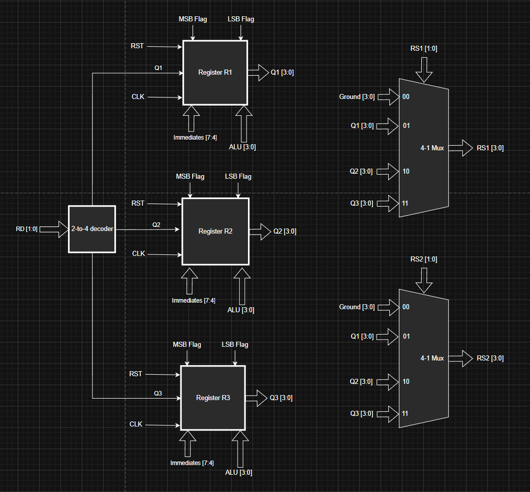
Note: for the case of R0 (Register 0 with value always being 0), it is a special case. Instead of using physical registers, R0 is effectively always zero by wiring ground to R0 input on ALU's mux.
For any register R1,R2,R3 (denoted as RN), it's circuit diagram is as follows:

Note: QN denotes the repsective Q-signal (output from 2-4 decoder for register RN). For S[1] and S[0] it denotes the MSB and LSB for the MUX select lines respectively.
Here's justification on why the control circuit for the mux select lines:
-
For S[1], it only needs to be "1" if the register is a target register, the register is storing value from a Move or Add/Sub instruction, and if reset phase is done. Hence, we only need AND gates. For MSB Flag, we assume control circuit can properly flag for Opcodes that indicate the instruction is Move, or Add/Sub.
-
For S[0], after the reset state, it should be a "1" when maintaining register value (when instruction does not write to the register at upcoming clock tick) or when its slected for instruction Add/Sub. Hence, RST signal is anded to create a bit-mask for reset phase, while we complement select so if register is not selected, it will always at non-reset phase result in S[0] = 1. If however, phase is still non-reset and the register is selected, LSB flag must be able to flag for Add/Sub instruction.
4) ALU design
Here is the implementation of the ALU:

*The overflow/underflow flag bits aren't shown in high-level diagram since the outputs only go to indicator leds.
Note: the indicator led is only useful to indicate overflow and underflow if next instruction to run is ADD or SUB respectively. Otherwise the output value is garbage in relation to your instruction.
5) Control Circuit design
Control circuit is required to ensure registers (PC and data) transition to the right state while ALU outputs according to the given ALU instruction (ADD/SUB).
Below, is the implementation of the control circuits component:

Note: most of the control signal being just wire from the output of my "Instruction data" signal is the result of properly formatting the binary encoding of the ISA. Its possible to do a arbitary encoding but it will make the control circuit very complex.
From part 2), for the MSB and LSB flag circuit, it is the decoder circuit that tells the register file based on current instruction's opcode, what should the mux's 2-bit select lines be.
Here's how the decoder design is justified (Karnaugh map is used to synthesize the circuit):
-
For MSB, from Part 2), it needs to flag for instruction Move, ADD, and Sub. For Add and Sub, "Instruction data [1]" bit is always "1" while for move "Instruction data [0]" bit is always [1]. Hence, we simply need to check either "Instruction data [1]" or "Instruction data [0]" is "1" to only reject the jump instruction
-
For MSB, from Part 2), it needs to flag for instruction Jump, Add, and Sub. For Add and Sub, "Instruction data [1]" bit is always "1" while for Jump, all "Instruction data" bits are "0". Hence, we can simply detect if either "Instruction data [1]" bit is "1" or "Instruction data [0]" bit is "0".
6) Programming I have written a test program to test out the CPU.
# comments include (Instruction data [7:0])
# this ISA is defined for my specific CPU. It is not a common ISA like ARM64 or RISC-V.
Add R0 R0 R0 #(00 00 00 11) does no operation at start of PC 0x0 (R0 R0 R0 represents RD, RS1, and RS2 respectively)
Move R1 6 #(01 10 01 01)
Move R2 8 #(10 00 10 01)
Move R3 4 #(01 00 11 01)
Add R3 R1 R2 #(01 10 11 11)
Sub R1 R1 R2 #(01 10 01 10)
Add R2 R1 R0 #(01 00 10 11)
Jump 1 #(00 01 00 00)
7) Demo
This Youtube link will show progress of the build and the demo of the test program.